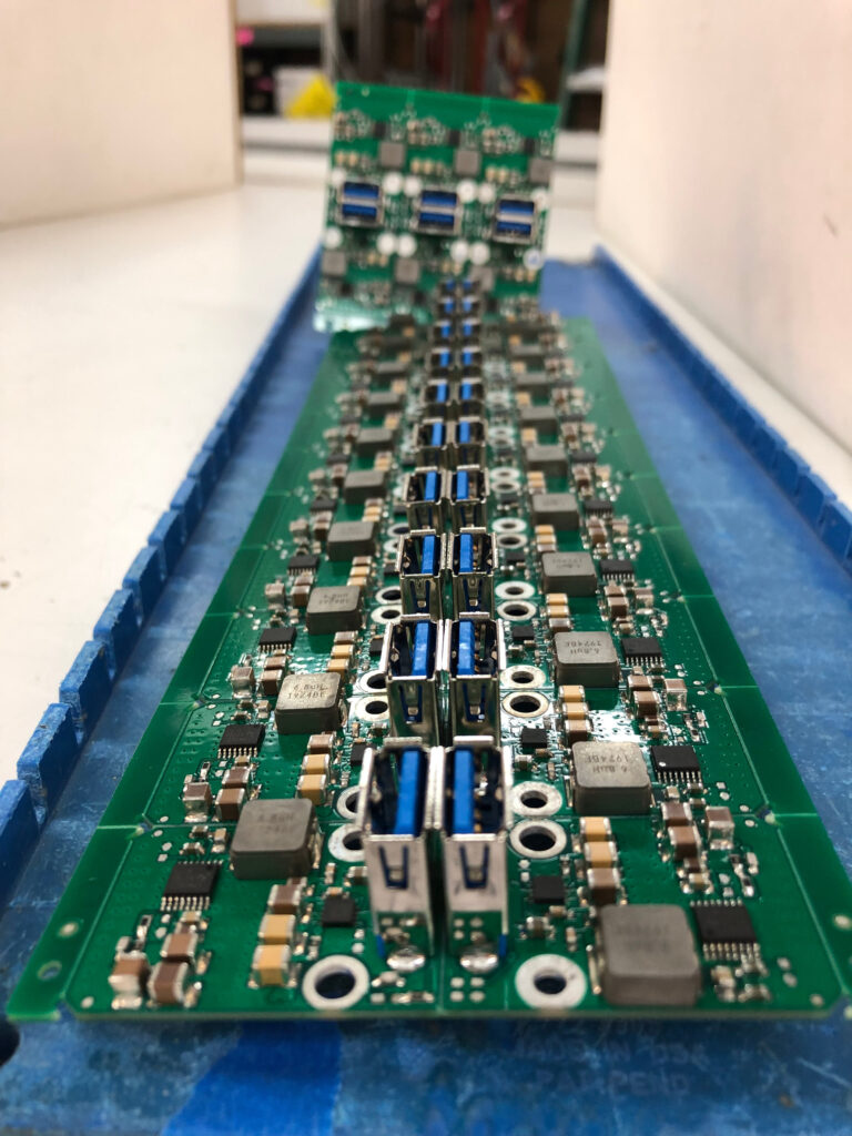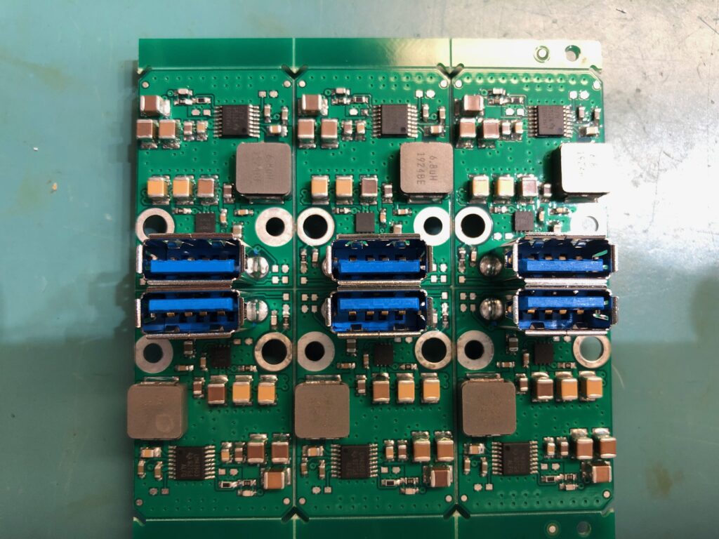
These USB power devices were hard to solder well. The four layers of ground planes and no thermal relief caused some areas to get too hot or other areas to not flow well.
The original designer didn’t have the bandwidth to help and didn’t have the original design files for us to work off of.
We reverse engineered the PCB so that we have the whole project now in Altium where we can easily make changes.
It was then a simple matter of adding a rule for thermal relief, wasn’t it?
Nope! Simply adding thermal relief to the design as-is would’ve made some power traces to filtering caps too small to effectively filter out the ripple and lower EMI. We added additional traces on other layers to lower the impedance.
During our changes we also discovered several ways to reduce the BOM cost by several dollars and count by a few parts. These boards are being produced in the 100’s. All of that savings could add up into a lot of profit. Unfortunately, we had to delay those changes for now because this project had both time constraints and extra vetting would need to be done since it is being used in aerospace.
See if we can help you make your design easier to manufacture!